Exhibition dates September 2–4, 2026
Venue TaiNEX, Taipei Booth T9508
YONATA Electronics showcased test solutions at SEMICON Taiwan 2026.
Through on-site displays and face-to-face discussions, the team introduced testing applications across silicon photonics wafers, optoelectronic bare dies and CPO modules.
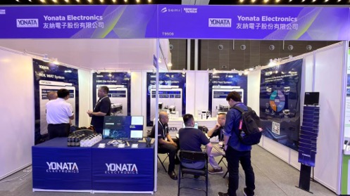
YONATA’s booth featured optoelectronic test solutions and on-site discussions with industry visitors.
The exhibition focused on testing and validation for integrated optoelectronic devices.
From initial wafer screening and bare-die verification to module-level system testing, YONATA presented the capabilities and application value of each stage.
The three technical areas are outlined below.
Silicon Photonics Wafer Testing
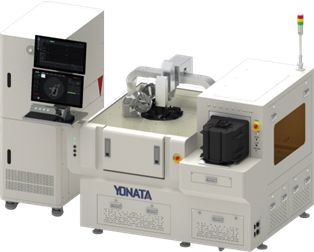
- Optical and electrical testing: O/O, O/E and E/E testing supports initial wafer-level screening.
- Coupling flexibility and repeatability: Vertical and edge coupling with fast alignment and coupling repeatability below 0.2 dB.
- Wafer and temperature compatibility: Supports 6- to 12-inch wafers and test temperatures up to 150 °C.
- Changeover and workflow integration: Quick probe-card and fiber-array-unit (FAU) changes, fast calibration and MES integration.
Optoelectronic Die-Level Testing
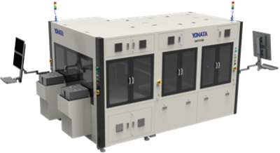
- Dual-side probing and active coupling: Top-side electrical and bottom-side optical probing, with grating coupling (GC) and edge coupling (EC), supports known-good-die (KGD) verification.
- Parallel testing and temperature control: Up to four parallel test sites and a test temperature range of 25–85 °C.
- Inspection, cleaning and traceability: Six-side AOI, automatic probe-tip cleaning and OCR support visual inspection and device traceability.
CPO Module Functional Testing
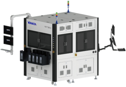
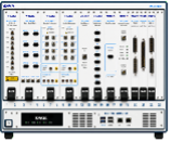
- Full-system testing (SLT): System-level functional verification for CPO modules.
- Optical loopback: Optical loopback testing verifies module signal transmission.
- Electrical and optical interfaces: Electrical sockets and optical connections support module-level testing.
On-Site Discussions and Further Collaboration
Through display panels, exhibits and technical explanations, the YONATA team discussed optoelectronic testing applications with customers and industry visitors.
These face-to-face conversations connected test solutions with application needs and created opportunities for further technical evaluation and collaboration.
Thank you to everyone who visited the booth.
Contact YONATA to discuss test solutions and application requirements.
Contact YONATA
About YONATA
Headquartered in Tokyo, Japan, YONATA Electronics provides advanced semiconductor test solutions combining high-speed optical and electrical signal processing, high-precision analog measurement, and wafer- and die-level automated handling. Serving applications including CPO, silicon photonics and chiplets, the company supports customers from technical consultation and test planning through system implementation, with a presence in Hsinchu, Taiwan.